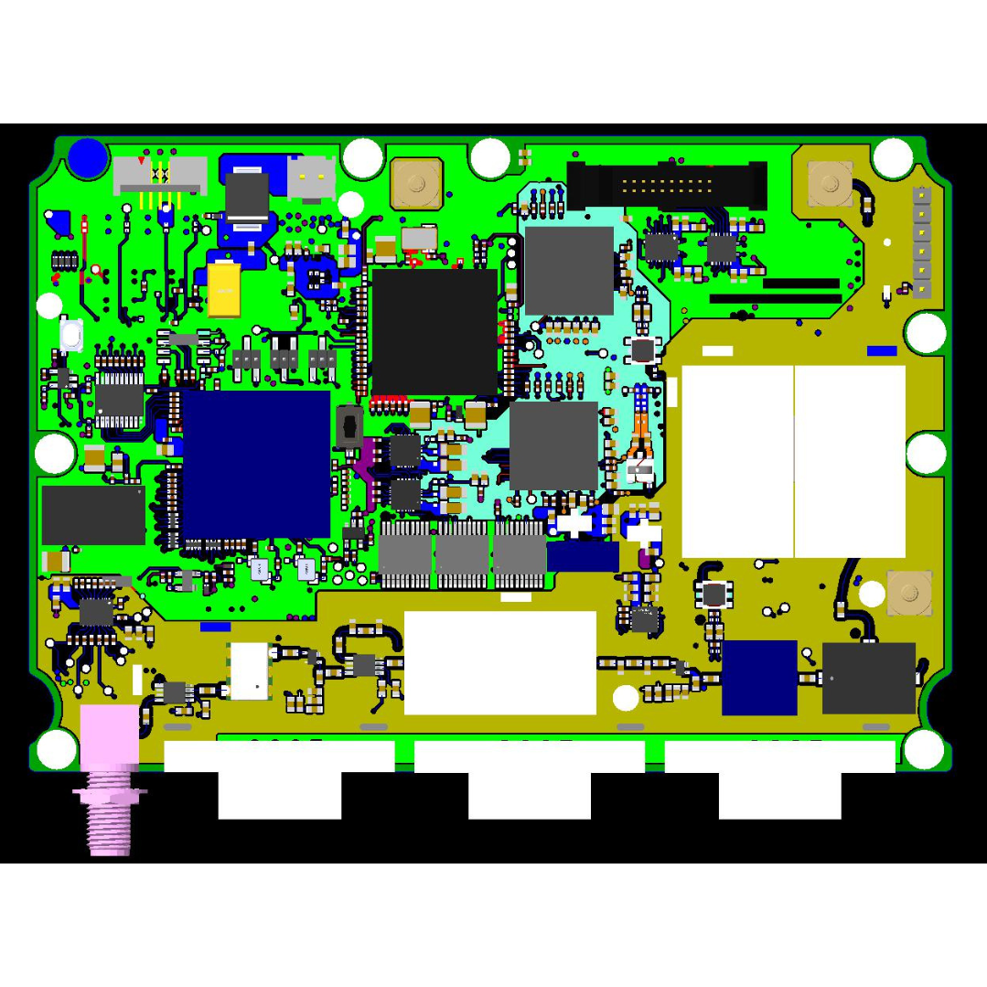
This case study showcases General Datum’s successful design of a compact, high-density 18-layer Baseband + RF card for aerospace and defence. Integrating RF and high-speed digital circuits (up to 1 GHz) within strict size and height constraints, the project highlights our expertise in delivering reliable, SWaP-optimized HDI solutions.
Industry: Defence Satellite Communication
Why us?
PSUs, defence, and aerospace organizations choose General Datum for our proven expertise in complex, high-reliability mixed-signal PCB design. We leverage simulation-driven approaches and strong DFM practices to achieve first-pass success while meeting stringent SWaP and MIL-grade requirements. Our track record with leading Indian defence entities reflects our ability to deliver high-quality, cost-effective solutions within tight timelines—making us a trusted partner for mission-critical systems.
Challenges
Faced significant challenges due to tight board size, height restrictions, and dense integration of RF, high-speed digital, and power circuits within a compact form factor.
Key issues included:
Limited routing space causing EMI, crosstalk, and signal integrity risks
Complex fan-out for fine-pitch components
Managing thermal performance, clean power delivery, and high-frequency signals simultaneously
Ensuring manufacturability without increasing layer count or cost
Solutions
Adopted a simulation-driven HDI design approach to overcome size and height constraints. Optimized footprints and custom libraries improved placement and routing efficiency, while via-in-pad, blind, and buried vias enabled compact, high-density integration.
Clear domain partitioning and an optimized stack-up minimized EMI and crosstalk across RF, digital, and power sections. Comprehensive SI, PI, and thermal simulations ensured reliable power delivery, strong signal integrity, and effective heat management within the compact design.
Results
Achieved first-pass success, delivering a compact, high-performance PCB that met all electrical, thermal, and mechanical constraints.
Key outcomes:
Excellent signal integrity, stable power delivery, and strong EMI control across RF and digital domains
Effective thermal management for long-term reliability
Optimized via structures improving manufacturability and yield
No increase in layer count or cost despite high complexity
The final design is a SWaP-optimized solution, showcasing General Datum’s expertise in high-density, mixed-signal HDI PCB design for demanding aerospace and defence applications.